Head to page 50 of the latest Compound Semiconductor Magazine Volume 29 Issue 7 to see their review of Silanna’s Applied Physics Letters SPSL paper!
https://data.angel.digital/pdf/Compound_Semiconductor_Issue_7_2023.pdf
–
MBE for far-UV LEDs
150 mm sapphire substrates are a promising platform for high-volume production of far-UVC LEDs via MBE
WHILE MOCVD is the most common growth method for producing far-UV LEDs, MBE also enables high-volume, high-yield production of these devices, says Silanna UV.
This Australian outfit has made more than 10,000 functional devices from a 150 mm GaN-based epiwafer, produced on a sapphire substrate using a Veeco GEN200 MBE tool. Following packaging, these far-UV LEDs produce an output power of 1.7 mW at peak efficiency, and have a lifetime of several thousand hours.
Silanna’s devices are compelling candidates for the optical source for disinfection and sterilisation. Emitting below 240 nm, radiation from these LEDs has minimal penetration beyond the outmost layers of skin, ensuring that exposure poses a reduced cancer risk. In addition, the company’s far-UVC LEDs can be used in sensing and high-performance liquid chromatography.

These far-UVC LEDs are produced on commercial 150 mm sapphire substrates, which are outgassed prior to growth in the Veeco GEN200.
“The Veeco GEN200 platform is a dual-chamber system, so we are capable of meeting current demand,” says Jordan Nichols, a senior device integration engineer at Silanna, who reveals that the company’s epitaxy facility has been purpose built to expand production capacity as demand grows.
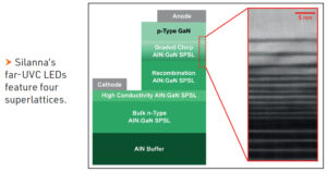
To form the LED’s epistructure, Silanna’s engineers deposit a 400 nm-thick AlN buffer, followed by four different superlattices and then a p-type GaN layer (see Figure). The superlattice for the recombination region is about 80 nm-thick and features 36 periods, with layer widths tuned to meet the target wavelength, which can vary from 229 nm to 240 nm.
“Devices at shorter wavelengths will have a lower output power,” says Nichols. “We bin our LEDs to assist customers with selecting the appropriate output power and wavelength for their desired application.”
One merit of using a short-period superlattice for the active region is a band structure that promotes transverse electric emission, leading to increased light extraction efficiency. This form of active region also reduces the dopant ionisation energy, thereby reducing resistivity, compared with a conventional quantum well region for a far-UVC LED.
To improve hole injection into the heart of the device, Silanna inserts a chirp superlattice between the p-type GaN layer and the active region. Also acting as an electron-blocking layer, this chirp superlattice prevents electrons from overshooting the recombination region.
Silanna produces LEDs from its epiwafers using standard photolithography and metallisation processes. After forming mesas by dry etching,
Ti/Al contacts are deposited to form electrical contacts. Following the addition of a standard passivation layer, engineers at the company may undertake optoelectronic measurements at the wafer-level using an integration sphere.
Wafer-level maps of electroluminescence spectra were recorded for more than 10,000 individual LEDs driven at 20 mA. For these devices, emitting at around 233 nm, the standard deviation in peak wavelength for devices in the middle 100 mm of the wafer is just 0.16 nm, and the average optical power 0.2 W.
Nichols his co-workers have produced packaged LEDs by dicing 1 mm by 1 mm devices from epiwafers, thinning the substrate to 275 μm and polishing it, and then flip-chip bonding the die to an AlN ceramic package. These devices delivered a peak wall-plug efficiency of 0.55 percent at 50 mA. Cranking the current up to 1 A caused the output power to climb to 17.4 mW, which is claimed to be the highest radiant flux for a far-UV LED grown on sapphire.
Lifetime tests on 80 packaged devices driven at 20 mA indicate a lifetime of 2,800 hours, based on the time it takes for the radiant flux to decrease to 70 percent of its initial value.
Goals for the team include realising even higher output powers and longer wavelengths.
REFERENCE
J. Nicholls et al. Appl. Phys Lett. 123 051105 (2023)