

Silanna UV Partnership With Marktech at Photonics West
News Highlights
- Silanna UV adds Marktech Optoelectronics as a distribution partner
- Joint booth at Photonics West 2024 in San Francisco
- Silanna’s innovative 235nm and 255nm UVC LEDs highlighted
- New deep and far UVC LEDs enable new applications
- A safer, greener, more efficient UVC source
- Applications in hygiene, health, and chemical or material sensing
Silanna UV and Marktech Optoelectronics to Demo New UVC LEDs at Photonics West 2024
Partnering on Better Far UVC and Deep UVC LEDs for Germicidal UV, Chemical Sensing
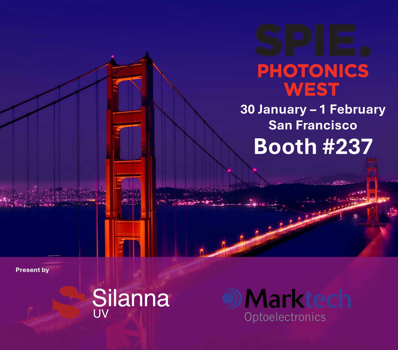
Brisbane, Australia, 16th January, 2024 – Silanna UV will unveil a new distribution partnership at Photonics West 2024. At the key US event, Silanna will share a booth with experienced US-based manufacturer, Marketch Optoelectronics, to celebrate Marktech commencing distribution of Silanna’s cutting-edge 235nm and 255nm UVC LEDs.
These new UVC LEDs enable safer, more eco-friendly, lower-power germicidal UV solutions, and chemical or material sensing. Photonics West 2024 runs from January 30 to February 1, 2024 in San Francisco. Silanna and Marktech will be in booth #237.
“Marktech Optoelectronics is one of the world’s leading manufacturers of UV, visible, near-infrared, and short-wavelength infrared (SWIR) emitters and detectors. With over 38 years of experience, they've assisted customers in designing best-in-class solutions for a variety of applications,” said Rob Lobban, Silanna UV’s Managing Director. “The partnership with Silanna UV isn't just a collaboration; it’s a strategic alliance to deliver cutting-edge far UVC solutions to the world. Silanna UV believes this partnership can revolutionize germicidal UV and chemical sensing by harnessing the two companies’ expertise.”
Innovative UVC LEDs Enable New Applications
At Photonics West, Silanna UV will be showing UVC products including the innovative SF1 235nm series and SN3 255nm series, which are making new UV products and applications possible in fields such as sterilization, water and gas sensing, and instrumentation. These UVC LEDs are available in flat or dome (parabolic) lens SMD format, or in TO-cans ball lens packages.
The SMD packages are a small footprint component with two lens options that provide wide or narrow UV coverage angles suitable for a variety of sensing and germicidal applications. The TO-can (Transistor Outline) format consists of a hermetically-sealed package, protecting sensitive components, with a ball lens that creates a narrow UV beam angle for the high irradiance required in most sensing applications. Marktech can also provide Silanna’s 235nm and 255nm LEDs in custom packaging.
Partnership to Broaden Customer Options
“We are very excited to collaborate with Silanna to expand our UVC product offerings via the Silanna SafeTM UVC solutions product portfolio, said Mark Campito, CEO of Marktech Optoelectronics.
“With almost four decades of providing optoelectronic solutions, Marktech has the expertise to identify and capitalize upon industry-changing technology such as Silanna UV’s innovative 235nm and 255nm UV LEDs. It is the perfect complement to our own wide range of optoelectronics product offerings.”
Silanna UV and Marktech look forward to meeting visitors at booth #237 at Photonics West 2024 in San Francisco where they can learn more about innovative deep UVC LED and far UVC LED solutions. Representatives of both companies will be available to answer questions and provide technical support.
Learn more about Silanna UV’s 235nm and 255nm UVC LED products at: https://silannauv.com/products/
About Silanna UV
The Silanna Group is an Australian semiconductor manufacturer established in 2006. Privately funded since being acquired from Peregrine Semiconductor in 2008, Silanna UV is an ISO 9001:2015 certified solution provider for UVC LED manufacturing. Based in Brisbane, Australia, Silanna UV provides far UVC light sources for water quality sensors, gas sensors, disinfection, and HPLC (High-performance liquid chromatography) applications. Silanna UV’s innovative approach allows UV LED technology to push toward shorter wavelengths, from 230nm to 265nm, including deep UVC and far UVC ranges. The company holds unique epitaxy technology and holds patents related to UV LED technology. With its unique UV LED technology, Silanna UV strives to create new possibilities by pushing UV wavelength boundaries to the limit.
To learn more, please visit http://www.silannauv.com/
Photonics West 2024
Hosted in San Fransico, USA
https://spie.org/conferences-and-exhibitions/photonics-west#_=_
Silanna UV will give a join exhibition with Marktech Optoelectronics at Photonics West 2024 San Francisco, USA (Booth: 237)
Jan 30th to Feb 1st, Silanna UV will proudly Exhibit at Photonics West 2024 in San Francisco, USA. Silanna UV will unveil a new distribution partnership at Photonics West 2024. At the key US event, Silanna will share a booth with experienced US-based manufacturer, Marketch Optoelectronics, to celebrate Marktech commencing distribution of Silanna’s cutting-edge 235nm and 255nm UVC LEDs.
Photonics West is the world’s leading photonics technologies event. Join the world’s largest photonics technologies event. Learn the most cutting-edge research in biomedical optics, biophotonics, industrial lasers, optoelectronics, microfabrication, MOEMS-MEMS, displays, quantum technologies, and more. Please join Silanna UV for this exciting event.
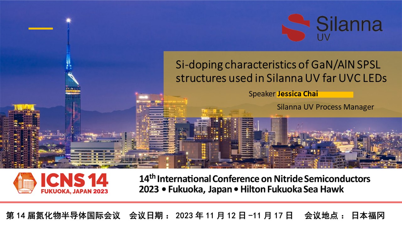
Silanna UV to Present New UV-C LED Manufacturing Technology at ICNS-14, Japan
News Highlights
- New UV-C LEDs allow more effective disinfection
- Silanna to present details at key Nitride Semiconductor conference
- Silanna executive to make presentation on manufacturing process
- Technology is safer with longer lifetime at lower power
- Patented GaN/AlN SPSL nanostructure manufacturing tech
- Silanna UV-C LEDs achieve 236 nm 18 mW at 1 Amp
-
Silanna UV to Present New UV-C LED Manufacturing Technology at ICNS-14, Japan
New Sub-240nm LEDS Are Safe, Effective, Power-Efficient, and Durable
Brisbane, Australia, 2nd November, 2023 – Silanna UV will reveal details of its unique new Far UVC LED manufacturing technology at the 14th International Conference on Nitride Semiconductors (ICNS-14) in Fukuoka, Japan from November 12 to 17, 2023. This technology is a significant advance in safe, effective, low-maintenance and low-power disinfection processes for air, water, surfaces and other applications.
Jessica Chai, Silanna’s molecular beam epitaxy (MBE) Process Manager will give a talk at the conference in 15:15-15:30 Tuesday 14th November 2023 at Room “Navis C”. Jessica will explain the Si-doping characteristics of the GaN/AlN SPSL (short period superlattice) nanostructures used in Silanna UV’s innovative far UVC LEDs. She will also present test results to illustrate the characteristics and benefits of the manufacturing technology.
A Revolution in Contactless Sanitization
Far UV-C LEDs are now acknowledged as a groundbreaking method of safe and effective contactless disinfection. Sub-240nm LEDs are of particular interest, because light below 240 nm inactivates pathogens while being safer in inhabited environments, compared to longer UVC wavelengths.
The traditional bulk AlGaN methods of producing high-Al AlGaN for far UV-C wavelengths suffer from multiple challenges. Silanna UV’s unique, patented III-Nitride SPSL technology overcomes these challenges. The company has successfully demonstrated sub-240nm far UV-C LEDs that achieve 236 nm 18 mW at 1 Amp on a flip-chip device.
More details of Silanna’s Far UVC LEDs at: https://silannauv.com/products
About Silanna UV
The Silanna Group is an Australian semiconductor manufacturer established in 2006. Privately funded since being acquired from Peregrine Semiconductor in 2008, Silanna UV is an ISO 9001:2015 certified solution provider for UV-C LED manufacturing. Based in Brisbane, Australia, Silanna UV provides far UV-C light sources for water quality sensors, gas sensors, disinfection, and HPLC (High-performance liquid chromatography) applications. Silanna UV’s innovative approach allows UV LED technology to push toward shorter wavelengths, from 230nm to 265nm, including deep UV-C and far UV-C ranges. The company holds unique epitaxy technology and holds patents related to UV LED technology. With its unique UV LED technology, Silanna UV strives to create new possibilities by pushing UV wavelength boundaries to the limit. To learn more, please visit http://www.silannauv.com/
ニュースハイライト
- 新しいUV-C LEDにより、より効果的な殺菌が可能に
- Silannaは窒化物半導体の主要会議で詳細を発表予定
- Silanna社エグゼクティブが製造プロセスに関するプレゼンテーションを実施
- 低電力で長寿命、より安全な技術
- 特許取得済みのGaN/AlN SPSLナノ構造製造技術
- Silanna UV-C LEDは1Aで236nm 18mWを達成
Silanna UVが日本で行われるICNS-14にて新しいUV-C LED製造技術を発表
新しい240nm 以下のLEDSは安全で効果的、かつ省電力、耐久性に優れている
オーストラリア、ブリスベン、2023年11月2日 - SilannaUVは、2023年11月12日から17日まで福岡で開催される第14回窒化物半導体国際会議(ICNS-14)で、独自の新しい遠UVC LED製造技術の詳細を発表する。この技術は、空気、水、表面、その他の用途において、安全で効果的、低メンテナンスかつ低電力の殺菌プロセスを大きく前進させるものである。
Silannaの分子線エピタキシー(MBE)プロセスマネージャーであるジェシカ・チャイ(Jessica Chai)が、2023年11月14日(火)15:15-15:30、ルーム "Navis C "にて講演を行う予定だ。 ジェシカは、Silanna UVの革新的な遠紫外線(Far UV-C)LEDに使用されているGaN/AlN SPSL(短周期超格子)ナノ構造のSiドーピング特性について説明する。また、この製造技術の特性と利点を示すテスト結果も紹介する。
非接触型除菌の革命
遠紫外線(Far UV-C)LEDは現在、安全で効果的な非接触消毒の画期的な方法として認められている。240nm以下の光は病原体を不活性化する一方で、人の住環境ではUVCの長波長に比べてより安全であるため、240nm以下のLEDは特に注目されている。
遠紫外線(Far UV-C)波長用の高Al AlGaNを製造する従来のバルクAlGaN法はさまざまな課題に悩まされているが、Silanna UVの独特かつ特許取得済みのIII-窒化物SPSL技術はこれらの課題を克服している。同社はフリップチップデバイスで236nm 18mW、1Aを達成する240nm以下の遠紫外線(Far UV-C) LEDの実証に成功している。
Silanna社の紫外線(Far UV-C)LEDの詳細はhttps://silannauv.com/productsからご覧いただけます。
Silanna UVについて
Silanna Groupは2006年に設立されたオーストラリアの半導体メーカーです。2008年にペレグリン・セミコンダクター社に買収されて以来、個人出資で設立されたSilanna UVはISO 9001:2015認証を取得したUV-C LED製造のソリューション・プロバイダーです。オーストラリアのブリスベンを拠点とするSilanna UVは、水質センサー、ガスセンサー、殺菌、HPLC(高速液体クロマトグラフィー)アプリケーション向けに遠紫外線(遠UV-C)光源を提供しています。Silanna UVの革新的なアプローチにより、UV LED技術は230nmから265nmの短波長化へと進み、深(deep)UV-Cや遠(far)UV-Cの範囲も含みます。同社は独自のエピタキシー技術を有し、UV LED技術に関する特許を保有しています。独自のUV LED技術により、Silanna UVはUV波長の限界を押し広げ、新たな可能性の創造に努めています。詳細については、http://www.silannauv.com/をご覧ください。
Head to page 50 of the latest Compound Semiconductor Magazine Volume 29 Issue 7 to see their review of Silanna’s Applied Physics Letters SPSL paper!
https://data.angel.digital/pdf/Compound_Semiconductor_Issue_7_2023.pdf
-
MBE for far-UV LEDs
150 mm sapphire substrates are a promising platform for high-volume production of far-UVC LEDs via MBE
WHILE MOCVD is the most common growth method for producing far-UV LEDs, MBE also enables high-volume, high-yield production of these devices, says Silanna UV.
This Australian outfit has made more than 10,000 functional devices from a 150 mm GaN-based epiwafer, produced on a sapphire substrate using a Veeco GEN200 MBE tool. Following packaging, these far-UV LEDs produce an output power of 1.7 mW at peak efficiency, and have a lifetime of several thousand hours.
Silanna’s devices are compelling candidates for the optical source for disinfection and sterilisation. Emitting below 240 nm, radiation from these LEDs has minimal penetration beyond the outmost layers of skin, ensuring that exposure poses a reduced cancer risk. In addition, the company’s far-UVC LEDs can be used in sensing and high-performance liquid chromatography.
These far-UVC LEDs are produced on commercial 150 mm sapphire substrates, which are outgassed prior to growth in the Veeco GEN200.
“The Veeco GEN200 platform is a dual-chamber system, so we are capable of meeting current demand,” says Jordan Nichols, a senior device integration engineer at Silanna, who reveals that the company’s epitaxy facility has been purpose built to expand production capacity as demand grows.
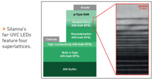
To form the LED’s epistructure, Silanna’s engineers deposit a 400 nm-thick AlN buffer, followed by four different superlattices and then a p-type GaN layer (see Figure). The superlattice for the recombination region is about 80 nm-thick and features 36 periods, with layer widths tuned to meet the target wavelength, which can vary from 229 nm to 240 nm.
“Devices at shorter wavelengths will have a lower output power,” says Nichols. “We bin our LEDs to assist customers with selecting the appropriate output power and wavelength for their desired application.”
One merit of using a short-period superlattice for the active region is a band structure that promotes transverse electric emission, leading to increased light extraction efficiency. This form of active region also reduces the dopant ionisation energy, thereby reducing resistivity, compared with a conventional quantum well region for a far-UVC LED.
To improve hole injection into the heart of the device, Silanna inserts a chirp superlattice between the p-type GaN layer and the active region. Also acting as an electron-blocking layer, this chirp superlattice prevents electrons from overshooting the recombination region.
Silanna produces LEDs from its epiwafers using standard photolithography and metallisation processes. After forming mesas by dry etching,
Ti/Al contacts are deposited to form electrical contacts. Following the addition of a standard passivation layer, engineers at the company may undertake optoelectronic measurements at the wafer-level using an integration sphere.
Wafer-level maps of electroluminescence spectra were recorded for more than 10,000 individual LEDs driven at 20 mA. For these devices, emitting at around 233 nm, the standard deviation in peak wavelength for devices in the middle 100 mm of the wafer is just 0.16 nm, and the average optical power 0.2 W.
Nichols his co-workers have produced packaged LEDs by dicing 1 mm by 1 mm devices from epiwafers, thinning the substrate to 275 μm and polishing it, and then flip-chip bonding the die to an AlN ceramic package. These devices delivered a peak wall-plug efficiency of 0.55 percent at 50 mA. Cranking the current up to 1 A caused the output power to climb to 17.4 mW, which is claimed to be the highest radiant flux for a far-UV LED grown on sapphire.
Lifetime tests on 80 packaged devices driven at 20 mA indicate a lifetime of 2,800 hours, based on the time it takes for the radiant flux to decrease to 70 percent of its initial value.
Goals for the team include realising even higher output powers and longer wavelengths.
REFERENCE
J. Nicholls et al. Appl. Phys Lett. 123 051105 (2023)
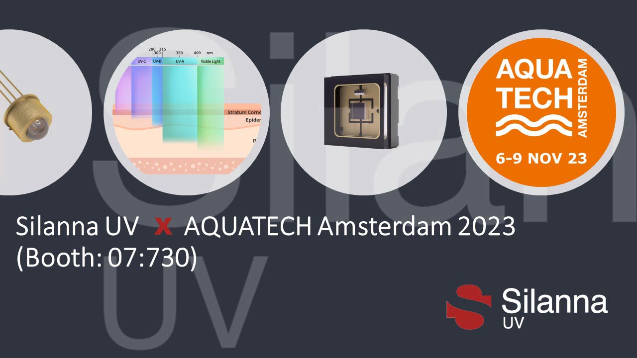
Silanna UV to Demo Innovative UV-C LED Water Quality Sensors at AQUATECH 2023
News Highlights
- Innovative UV-C water quality monitoring LED technology
- Detects Nitrates and organic compounds
- Rapid, accurate measurement
- Long lifetime
- Compact and cost-effective
- Safe for users
- Mercury-free and environment-friendly
Silanna UV to Demo Innovative UV-C LED Water Quality Sensors at AQUATECH 2023
Detects Nitrates and Organics Rapidly – Environmentally Safe, Low Power, and Long Lifetime
Brisbane, Australia, 19th October, 2023 – Silanna UV will demonstrate innovative new technology for detection of nitrates and organic compounds in water at AQUATECH Amsterdam from November 6 to 9, 2023. Contamination of water by nitrates and organic compounds is a growing problem, and regulations to protect the public from this threat are increasingly stringent.
At AQUATECH, Silanna UV will showcase its SF1 series of Ultraviolet LEDs, which are ideal for water purity applications such as nitrate detection, organic compound detection, disinfection, and HPLC chromatography. Silanna UV is a pioneer in developing patented UV LED technology for shorter wavelengths, from 230nm to 265nm, including deep UV-C and far UV-C ranges.
The SF1 series achieves a peak wavelength under 235nm and a Full-Width-Half-Max (FWHM) peak of 10nm, which enables high sensitivity and accuracy for measuring low levels of dissolved nitrate and other contaminants in water. The SF1 series also offers a long lifetime of more than L50 >9,000hrs (>1 X 10⁹) measurements, a low power consumption of less than 0.12W, and a compact and robust design.
Better Technology for Cleaner Water
Nitrate contamination in drinking water can be harmful to humans, according to the United States Environment Protection Agency, the Minnesota Department of Health, and other respected organizations. With increasingly strong regulations that demand nitrate limits as low as 10mg/L-N, the need for monitoring and controlling dissolved nitrate is now a priority in water supply.
In traditional Nitrate and Nitrite detection, broadband light generated by a lamp is passed through an expensive spectroscopic pathway to extract only the far UV-C wavelength needed for sensing applications. However, this is complex, wastes power, and may require environmentally-harmful materials.
In contrast , narrowband UV light under 240nm is perfect for this application. Silanna’s SF1 series of LED UV-C emitters with peak wavelength under 235nm and a Full-Width-Half-Max (FWHM) of 10nm makes them an ideal candidate for a new generation of nitrate sensing devices.
Ready-To-Go Nitrate-Detecting Reference Design
At AQUATECH Silanna UV will demonstrate its nitrate-sensing reference design, which uses the 235nm SF1-3U8P3L1 UV LED emitter in a parabolic lens package that produces a quasi-collimated far UV-C beam.
The reference design detects dissolved nitrate in a water sample in only 0.5 sec, with effectively no warm-up delay. This reduces power consumption and allows high-precision results as frequently as once per minute for most applications. The results, including units of mg/L-N (PPM of Nitrogen in nitrate), are displayed instantly on the clear 2.8-inch touch screen. The reference design is cost-effective, power efficient, environmentally friendly, mercury-free, and incorporates a safety interlock to protect users from UV-C exposure.
In addition to nitrate detection, Silanna UV will also demonstrate the detection of organic compound contamination via Chemical Oxygen Demand (COD) and UV254 absorption tests. These tests help monitor water quality and prevent potential health risks from harmful substances such as pesticides, herbicides, pharmaceuticals, and industrial chemicals.
See the Future of Water Quality at the Show
AQUATECH Amsterdam 2023, the world's leading trade show for clean drinking water production and wastewater treatment, will take place from November 6th to 9th, 2023 at the RAI Amsterdam Convention Centre in Amsterdam, Netherlands.
Silanna UV will be at Booth 07:730.
Silanna UV invites all visitors to its booth to learn more about its innovative deep UV-C LED and far UV-C LED solutions for water applications and more. Silanna UV's application team will be available to answer any questions and provide technical support.
Further details of Silanna’s SF1 series are available at: https://silannauv.com/products/sf1-235nm-flat-lens/
About Silanna UV
The Silanna Group is an Australian semiconductor manufacturer established in 2006. Privately funded since being acquired from Peregrine Semiconductor in 2008, Silanna UV is an ISO 9001:2015 certified solution provider for UV-C LED manufacturing. Based in Brisbane, Australia, Silanna UV provides far UV-C light sources for water quality sensors, gas sensors, disinfection, and HPLC (High-performance liquid chromatography) applications. Silanna UV’s innovative approach allows UV LED technology to push toward shorter wavelengths, from 230nm to 265nm, including deep UV-C and far UV-C ranges. The company holds unique epitaxy technology and holds patents related to UV LED technology. With its unique UV LED technology, Silanna UV strives to create new possibilities by pushing UV wavelength boundaries to the limit. To learn more, please visit http://www.silannauv.com/